
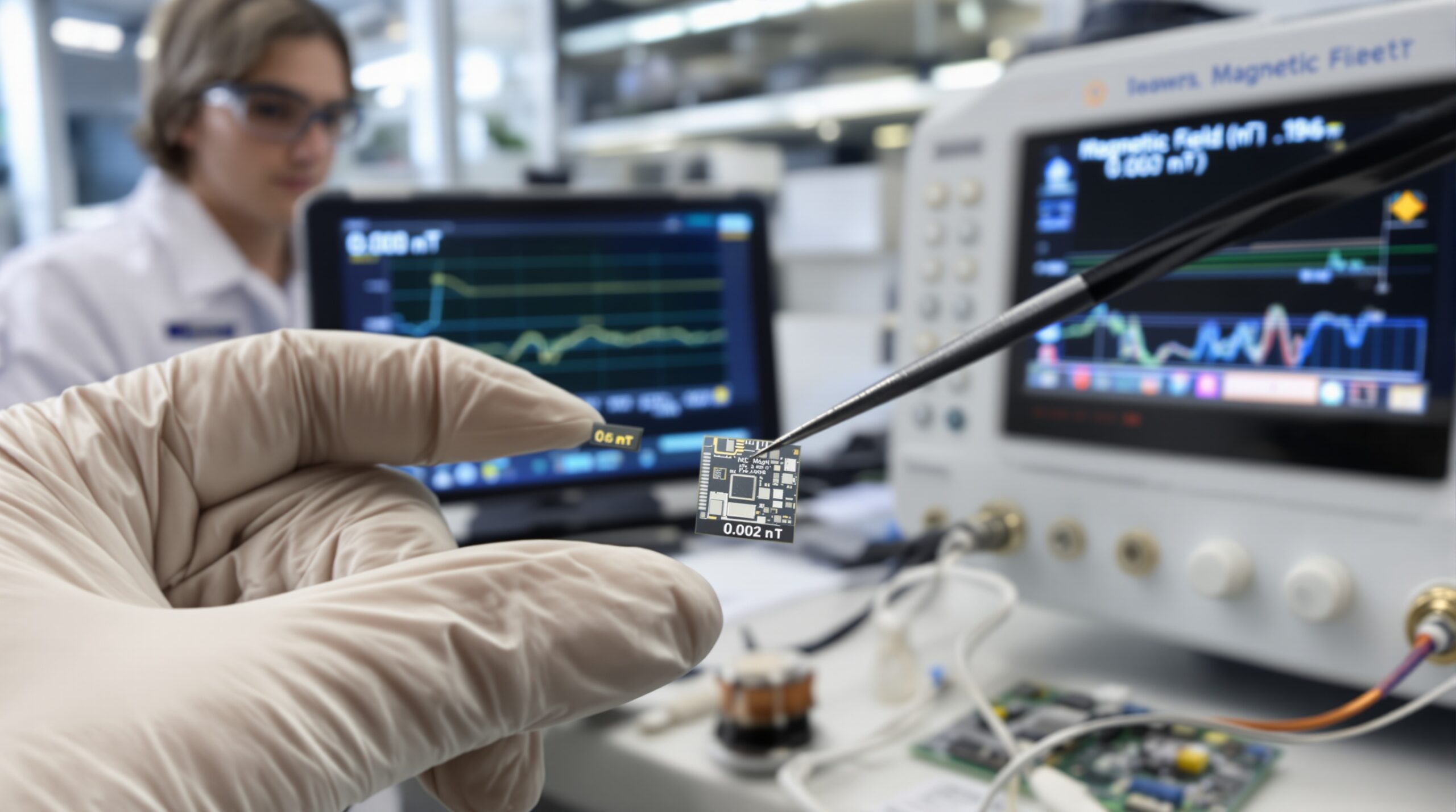
A new generation of room‑temperature quantum sensors is moving from lab benches onto tiny chips. Engineers have demonstrated nanotesla precision in a compact device that integrates light, control electronics, and sensing elements. The advance removes the need for cryogenics or bulky enclosures, which have limited quantum sensing adoption. It also aligns with growing demand for portable, low‑power medical and industrial instruments. This transition opens credible paths toward handheld imaging and rapid field diagnostics.
What the latest demonstration achieved
The reported chip‑scale quantum magnetometer operates at room temperature with nanotesla‑level sensitivity. The device integrates the active sensing medium, optical interfaces, and on‑chip control structures. Designers prioritized low power, compact packaging, and compatibility with standard semiconductor processes. They also addressed common noise sources with careful shielding and digital signal processing. These features collectively suggest a platform ready for portable instruments and distributed sensor arrays.
Why nanotesla sensitivity matters
Magnetic field strength spans an enormous range, from Earth’s field to tiny biological signals. A nanotesla is one‑billionth of a tesla, which represents a very small field. Many biomedical and materials signals fall in the nanotesla to picotesla range. Achieving nanotesla precision at room temperature enables measurements previously limited to shielded rooms or cryogenic sensors. This sensitivity level underpins practical low‑field MRI, magnetocardiography, and chemical analysis in real‑world settings.
How chip‑scale quantum sensors detect magnetic fields
Quantum magnetometers exploit atomic or defect spin states that shift in magnetic fields. A light source prepares and probes those states, while microwaves or radiofrequency fields manipulate them. Changes in fluorescence or transmitted light reveal the magnetic field with high precision. On a chip, integrated photonics and microfabricated structures handle the light efficiently. Different physical platforms implement this concept with distinct trade‑offs and operating requirements.
Solid‑state defects enable robust, compact sensing
Diamond nitrogen‑vacancy centers are a leading solid‑state approach for room‑temperature sensing. Their spin states respond to magnetic fields and can be optically addressed and read out. Thin diamond membranes or micro‑fabricated diamond structures couple to on‑chip waveguides. This approach offers durability, wide bandwidth, and compatibility with micro‑optics. It also supports vector magnetometry and nanoscale proximity sensing for surface‑adjacent targets.
Alkali vapor cells deliver exceptional baseline sensitivity
Optically pumped magnetometers use alkali vapor, such as rubidium or cesium, in microfabricated cells. Polarized atoms precess in magnetic fields, modulating light transmission through the cell. Carefully controlled temperatures and low‑noise optics yield excellent sensitivity at room temperature. Chip‑scale heaters and thermal isolation maintain stable operation in small packages. These sensors excel in low‑field regimes and can approach shielded‑lab performance in portable formats.
From proof‑of‑concept to integrated photonics
Recent progress leverages silicon photonics and advanced packaging to shrink optical components. On‑chip lasers, modulators, and photodiodes reduce alignment complexity and power draw. Wafer‑level bonding aligns sensing media with photonic circuits and shielding layers. Co‑design of optics, electronics, and thermal paths minimizes drift and environmental coupling. These steps transform delicate laboratory setups into manufacturable, robust sensor chips.
Portable MRI moves closer to reality
Low‑field MRI relies on sensitive magnetometers to detect weak nuclear spin precession signals. Nanotesla precision enables detection at microtesla to millitesla fields with appropriate sequences. Pre‑polarization and optimized gradients can compensate for lower field strengths. Chip‑scale sensors could sit close to the body, improving signal capture and comfort. Together, these capabilities support compact scanners for point‑of‑care imaging and triage.
New opportunities for field diagnostics
Outside hospitals, magnetic sensing supports rapid, non‑contact diagnostics and inspections. Magnetocardiography can monitor heart activity without direct skin contact or gels. Battery packs reveal internal faults through magnetic signatures during charge and discharge cycles. Geophysical surveys benefit from arrays of small, low‑power sensors with high sensitivity. Industrial nondestructive testing gains options for detecting stress, cracks, and corrosion through magnetic signals.
Understanding precision, sensitivity, and bandwidth
Reports often quote sensitivity in nanotesla per square‑root hertz. That metric describes noise floor versus measurement time. Precision reflects the smallest resolvable change under defined conditions and averaging. Bandwidth determines how quickly the sensor tracks changing fields. Balanced performance across these parameters supports both imaging and real‑time monitoring applications.
Key engineering challenges remain
Thermal fluctuations shift resonance frequencies and impact stability in small packages. Stray fields from electronics and urban environments raise the noise floor. Optical scattering and laser intensity noise reduce readout fidelity if unmanaged. Cross‑sensitivities to temperature, strain, or vibration complicate calibration in the field. Robust gradiometry, shielding, and digital filtering will mitigate these effects in final products.
How this compares with existing technologies
SQUID magnetometers deliver superb sensitivity but require cryogenics and heavy shielding. Fluxgate and Hall sensors are compact and inexpensive but lack nanotesla precision. Optically pumped magnetometers offer high sensitivity at room temperature with moderate size. Solid‑state spin sensors provide durability and chip‑level integration advantages. The new chip‑scale approach blends OPM‑like sensitivity with solid‑state practicality and manufacturability.
Design strategies that boost real‑world performance
Vector configurations measure multiple axes and reject common‑mode disturbances. Compact gradiometers subtract environmental noise by comparing two nearby sensors. On‑chip reference oscillators and locking schemes reduce drift and linewidth broadening. Advanced materials and coatings stabilize vapor cells and suppress wall collisions. Machine learning filters help distinguish signals from nonstationary, real‑world noise sources.
Path to clinical and industrial deployment
Clinical devices require rigorous validation, standardized protocols, and regulatory clearance. Portable MRI demands careful safety analysis of fields, gradients, and acoustic noise. Industrial instruments must meet electromagnetic compatibility and ruggedness standards. Supply chain readiness for lasers, wafers, and specialty materials supports scale. Field trials will refine procedures, calibrations, and user interfaces for non‑expert operators.
What to watch in the next development cycles
Expect continued improvements in sensitivity, stability, and power consumption. Chip‑scale laser integration will reduce size and cost further. Dense arrays will enable spatially resolved imaging without bulky gradient coils. Hybrid systems will combine magnetometers with ultrasound or optical modalities. Standardized interfaces will accelerate ecosystem growth and application diversity.
Why this milestone is strategically important
Room‑temperature nanotesla precision on a chip represents a practical threshold. Below this level, many biological and materials signals emerge clearly. Achieving it without cryogenics reduces barriers to deployment and maintenance. Integrating the optics and electronics reduces system complexity and alignment overhead. These advances collectively shift quantum sensing from specialty labs to everyday tools.
Conclusion: Toward ubiquitous magnetic sensing and imaging
The march toward portable quantum magnetometry is accelerating and pragmatic. Nanotesla precision at room temperature on a chip unlocks broadened use cases. Healthcare can gain point‑of‑care imaging, monitoring, and faster triage outside specialized facilities. Industry and research benefit from sensitive, deployable instruments for inspection and discovery. The next wave will refine reliability and scale manufacturing, turning prototypes into trusted devices.