

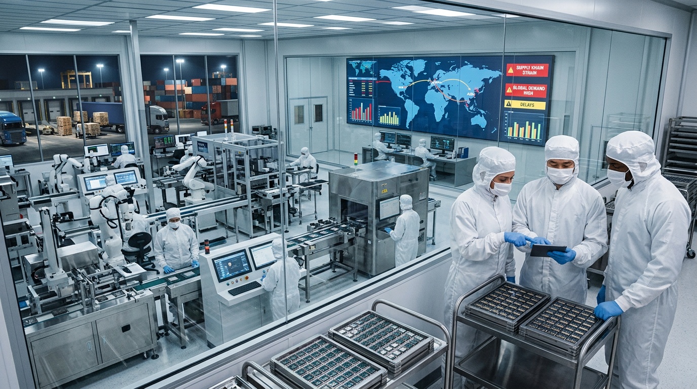
Artificial intelligence workloads keep exploding, and chipmakers are scrambling to keep pace. Training clusters demand unprecedented compute density, memory bandwidth, and energy efficiency. Traditional scaling delivers less benefit, so companies now lean on advanced packaging for performance gains. This shift stretches supply chains and creates urgent investment in new facilities. The race is global, capital intensive, and strategically vital.
Why Advanced Packaging Now Sits at the Center of AI
AI accelerators require fast links between compute dies and high bandwidth memory stacks. Advanced packaging shortens interconnects and raises bandwidth while improving energy efficiency. Technologies include 2.5D interposers, 3D die stacking, and chiplet integration schemes. These approaches assemble multiple dies into one functional system. Designers combine logic, memory, and I/O dies in tight proximity. The resulting modules outperform monolithic chips within today’s power and cost limits.
New approaches also diversify manufacturing tasks across several specialists. Foundries fabricate advanced logic dies, while OSATs assemble and test complex packages. Substrate makers supply high-density organic laminates for redistribution. Materials companies deliver underfills, resins, and interposer glass or silicon. The whole chain must scale together, or bottlenecks appear quickly. As AI demand surges, bottlenecks already shape product roadmaps and delivery schedules.
Capacity Constraints and Emerging Bottlenecks
Packaging capacity for AI accelerators remains tight despite rapid investments. Advanced interposers and 3D stacking require specialized lines with strict yields. CoWoS and Foveros processes face long cycle times and complex tooling requirements. High bandwidth memory assembly depends on through-silicon via and precise thermal control. These steps limit throughput and constrain launch volumes. Ramping capacity takes quarters, not weeks, given intricate equipment and training.
Substrates also present constraints, especially for large reticle-sized packages. Ajinomoto Build-up Film materials remain essential, and supply grows slowly. Substrate makers must expand capacity and improve fine-line capabilities. Lead times stretch as AI and networking customers compete for panels. Meanwhile, thermal solutions and power delivery challenge every design. Managing heat and current density drives co-design with cooling and boards. Integration complexity grows as modules scale beyond existing test capabilities.
Foundry Strategies to Expand Advanced Packaging
TSMC Accelerates CoWoS and SoIC Capacity
TSMC leads in 2.5D and 3D integration for AI accelerators. The company offers CoWoS for interposer-based assemblies and SoIC for 3D stacking. Demand from leading GPU and accelerator vendors strains capacity. TSMC has announced significant CoWoS expansions to serve AI customers. The company adds lines, tools, and skilled labor across multiple sites. These moves target increased monthly capacity through 2024 and 2025. Customers expect relief, though lead times remain meaningful. TSMC also evaluates advanced packaging options outside Taiwan to diversify risk.
Intel Scales Foveros and U.S. Assembly Investments
Intel continues ramping Foveros 3D stacking for disaggregated compute products. The company invested billions in New Mexico for advanced packaging lines. Additional assembly and test expansions proceed in Oregon, Arizona, and Malaysia. Intel positions advanced packaging as central to its foundry strategy. The roadmap emphasizes tiles, disaggregation, and high-density interconnects. These steps align with customer interest in chiplets and heterogeneous integration. Intel also works with OSAT partners to increase flexibility and coverage.
Samsung Pushes 2.5D, 3D, and HBM Integration
Samsung expands packaging capabilities to support AI logic and memory integration. The company promotes I-Cube and X-Cube for 2.5D and 3D assemblies. It has introduced SAINT for advanced 3D stacking with TSVs. Samsung aligns foundry and memory businesses to co-optimize HBM with accelerators. Packaging expansions in Korea target higher throughput and improved yields. The company courts hyperscalers and system companies seeking tight co-design. Efforts include design enablement for thermal and power delivery challenges.
OSAT Providers Build New Plants and Capabilities
Outsourced assembly and test providers now sit at the heart of scaling. ASE, Amkor, JCET, SPIL, and Powertech expand advanced lines worldwide. These companies add interposers, wafer-level packaging, and 3D stacking equipment. They also strengthen materials partnerships and substrate procurement. The goal is consistent output across several regional hubs. Customers value redundancy and geographic diversity after pandemic disruptions. OSATs therefore pitch resilience alongside technical competencies.
Amkor announced a large advanced packaging facility in Arizona. The site aims to support U.S. customers with local assembly and test. It plans to handle high-value modules, including AI and automotive products. Construction and tooling will proceed in phases as demand matures. This move complements Amkor’s existing Asian footprint and partnerships. Other OSATs increase investments in Taiwan, Malaysia, Singapore, and China. Collectively, these expansions seek to reduce lead times and improve service.
Memory Makers Ramp HBM Packaging for AI
High bandwidth memory remains foundational for AI training and inference. SK hynix, Samsung, and Micron all accelerate HBM roadmaps and capacity. Stacks grow denser with more layers and improved power efficiency. Packaging must deliver reliable TSV connections and strict thermal performance. Manufacturers invest in new lines for underfill, bonding, and test. Capacity additions target HBM3E and future generations with wider interfaces. Close collaboration with accelerator vendors reduces cycle time and tuning needs. Supply should improve, but demand still rises quickly across regions.
Substrate and Materials Supply Chains Remain Critical
Advanced packages rely on high-density substrates with very fine traces. Suppliers like Ibiden, Unimicron, Nan Ya, Shinko, AT&S, and Kinsus expand capacity. They work to shrink line widths and improve warpage control. Yield improvements matter because panels grow larger with AI packages. Materials partners refine ABF formulations for reliability and thermal stability. Resin and underfill suppliers optimize chemistries for stacked dies. Toolmakers deliver new exposure, plating, and inspection equipment. Investment cycles here determine overall system throughput and reliability. Delays at this tier can stall whole product launches.
Government Incentives and Strategic Localization
Governments view advanced packaging as economically and strategically important. The United States advanced funding under the CHIPS Act to spur localization. Europe launched its Chips Act to expand capacity and resilience. Japan offers subsidies to attract foundry and packaging projects. South Korea introduced tax incentives and policy support for semiconductor leadership. India promotes assembly and packaging investment with targeted programs. These efforts encourage regional plants and diversified supply networks. Companies increasingly blend global and local footprints for risk management. However, building talent pipelines remains a persistent challenge.
Technology Directions Shape Plant Design
Plant layouts now reflect chiplet-based architectures and heterogeneous integration. Facilities must handle wafer-to-wafer bonding and panel-based processes. Co-design emerges as a required discipline across silicon, package, and system. EDA vendors incorporate thermal, mechanical, and power integrity models earlier. Standards like UCIe aim to simplify die-to-die interfaces. Adoption could improve reuse and speed ecosystem growth. Test strategies also evolve to manage large multi-die assemblies. Inline inspection and advanced metrology help maintain yields at scale.
Thermals drive many decisions about materials and form factors. Advanced packages increasingly pair with liquid cooling and improved heat spreaders. Power delivery networks require thicker copper and careful via planning. Engineers co-optimize bump pitches, redistribution layers, and interposer routing. These choices influence substrate sourcing and delivery times. Manufacturers therefore push concurrent engineering across the supply chain. Effective collaboration can save months in a tight market.
Customer Implications and Delivery Timelines
Hyperscalers and system makers must plan further ahead than before. Securing capacity often involves multi-quarter commitments and co-investment. Forecast accuracy helps partners deploy tools and crews efficiently. Design changes late in development can ripple across suppliers. Thermal revisions may require new substrates or module reinforcements. Qualification then restarts, pushing schedules to the right. Early package co-design reduces rework and improves time to volume. Customers that engage deeply tend to secure better outcomes.
Pricing also reflects the capital intensity of advanced packaging. Equipment, cleanroom space, and training costs continue rising. Substrates and HBM components command premiums under tight supply. Vendors balance pricing with long-term relationships and roadmap alignment. Customers increasingly sign longer agreements to stabilize supply. These contracts support predictable investments in capacity and tooling. Financial visibility benefits both sides as the market remains dynamic.
Regional Diversification and Risk Management
Companies diversify sites to reduce geopolitical and logistical risks. Multi-region packaging strategies complement global wafer fabrication. Local assembly and test can shorten delivery routes and customs cycles. Redundancy also helps absorb shocks from natural events or outages. However, spreading operations adds coordination and inventory challenges. Digital twins and standardized processes ease cross-site replication. Quality systems and supplier audits remain essential elements. Effective governance keeps performance consistent across geographies.
Outlook: A Prolonged Build-Out to Meet AI Ambitions
Advanced packaging investment will continue throughout this decade. AI roadmaps require larger modules, denser stacks, and faster interconnects. Supply chains must grow in lockstep to meet schedules. Foundries, OSATs, and materials firms will collaborate more closely. Governments will extend incentives tied to local jobs and security. Training programs will expand to address skills gaps in packaging. Standard interfaces should unlock broader chiplet ecosystems over time. These developments will gradually ease bottlenecks and shorten lead times.
Nonetheless, volatility will persist as AI demand evolves quickly. Breakthrough models can shift hardware specifications within months. Suppliers must improve agility while protecting yields and reliability. Co-design and early capacity reservations remain the best defenses. Companies that integrate across silicon, package, and system will lead. Their plants will embody flexible lines, robust metrology, and strong partnerships. The global race is underway, and the winners will define computing’s next era.
